DesignSpark PCB Version 8.1 Has Been Released!
Follow article
 Dave from DesignSpark
How do you feel about this article? Help us to provide better content for you.
Dave from DesignSpark
Thank you! Your feedback has been received.
Dave from DesignSpark
There was a problem submitting your feedback, please try again later.
Dave from DesignSpark
What do you think of this article?
DesignSpark V8.1 is here! Featuring a whole host of the updates you have been chasing us to add to this incredibly versatile free-to-download PCB design software. Just for you, we’ve added: Zoom level increase, copper pour keepout areas, Eagle ‘native’ import and much, much more.
On the release date (or after), if you are using an older variant of the software, there will be a prompt to update your version of DSPCB to version V8.1 (if you haven’t already), users downloading the software for the first time will receive the latest version. Simply update as required to ensure you are getting the best experience out of your PCB design software.
Version 8.1 contains all these improvements:
Zoom Level Increase
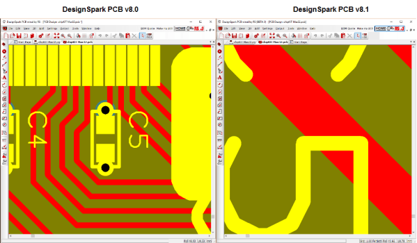
The maximum zoom level has been increased by a factor of 8. This will allow you to zoom-in further to inspect critical areas/items in your designs.
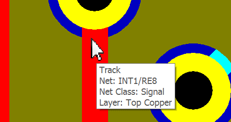
Tooltips includes Net Class Name
The Net field on design tooltips now includes Net Class Name (if defined).
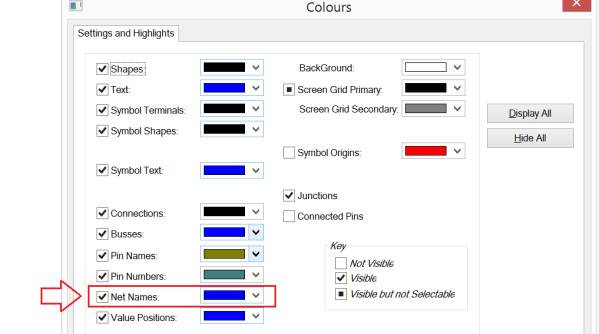
Display of Net Names in schematic
From within the Display dialogue, Settings & Highlights page, you can now switch off Net Names using the new checkbox as well as being able to just select the colour for Net Names.
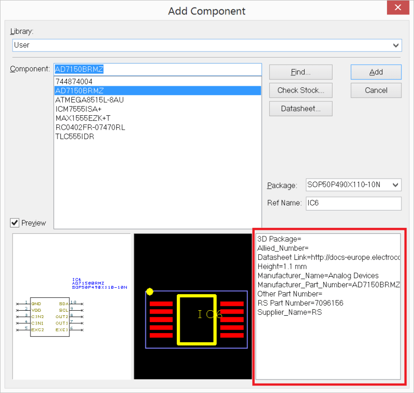
Add Component - Values Preview
On the Add Component dialogue, a new list of the Component Values is displayed in a box to the right of the existing Schematic and PCB symbol Preview windows. This will further help you confirm the chosen component is the correct one before you add it to your design.
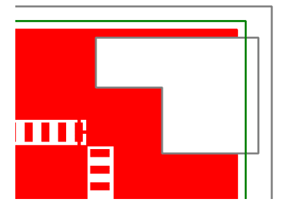
Copper Pour Keepout Areas on Power Planes
Adding a Copper Pour Area to a power plane layer and designating it as a Pour Keepout will cause that region of the layer to be kept clear of copper on the resulting plane.
To designate the Copper Pour Area as a Keepout Area, select the area and then in Properties, select the Pour Keepout check box.
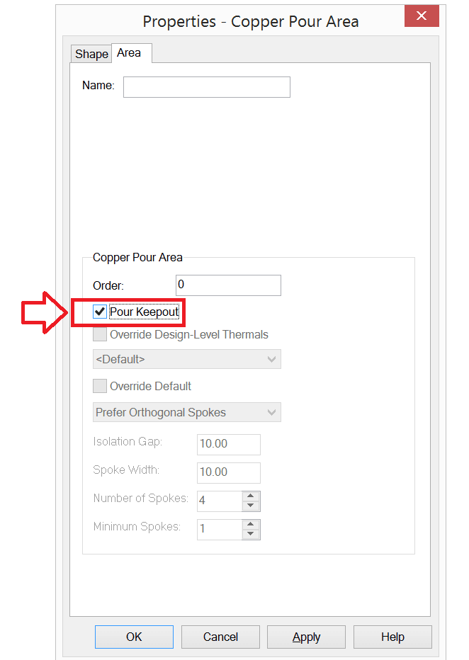
*When the Pour Keepout area is added to the design layer, copper is not added to that area when poured.
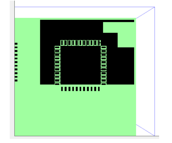
The area will be shown on the Preview in the Plotting & Printing dialogue to assist you in checking that the area is set up correctly.
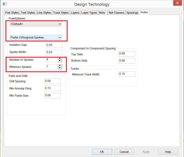
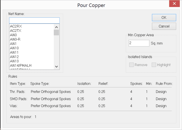
Improved control of thermal connections can be found in the Rules tabs of the Design Technology dialogue
There is an expanded definition of rules for thermal relief in Pour Copper and Powerplanes. The extra settings at design level (defined in Design Technology and Rules) allow the number of spokes, minimum spokes, spoke direction, isolation gap, and thermal relief width to be set for all items, and optionally over-ridden for plated through hole pads, SMD pads, and vias. The same set of thermal rules is available per Area if required. These design-level rules can also be overridden in the Copper Pour Area Properties (see below).
Pour Copper Changes (PCB)
When using the Pour Copper dialogue, if the parameter selection dialogue has been changed. It will now show you the rules that the Pour Copper function will use.
Changes to Area Properties (PCB) Copper Pour Areas
Below shows the Properties dialogue for Copper Pour Areas. This has been implemented to allow for the expanded controls for thermal rules per area.
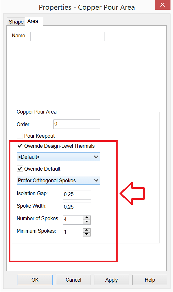
Checking the Override Design-Level Thermals will allow you to add specific thermal properties to individual areas. This overrides the settings defined in the Design Technology within the Rules tab.
Eagle ‘native’ import
The standard Cadsoft Eagle design and library import mechanism have been improved with the introduction of ‘native’ format import. This means an Eagle file does not need to be converted now to import it into DesignSpark PCB making the process much easier.
To convert Eagle files, simply drag the .sch or .brd file from Windows Explorer to the open DesignSpark PCB program. The standard import dialogue will be displayed to confirm the file format. You can choose to import the file using a Technology file at this point also.
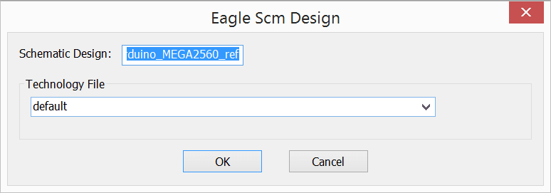
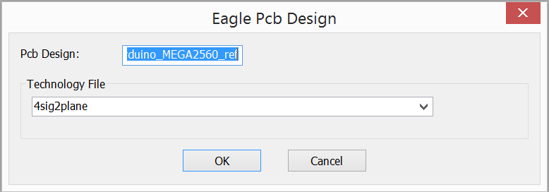
Note: files older than Eagle V6 must still be imported using the previous Eagle intermediate ULP format files which are still available.
Additional characters allowed in component names
Components in a design can now be named using more than just alphanumeric characters. Up to now, you had to name them with alphabetic first and alphanumeric for the rest. Now it will allow you to use alphanumeric anywhere, plus any of the following, in any order:
- _ $ £ & + = ! @ # ~ \ /
Note: only use these special characters if you are fully aware of the implications of doing so.
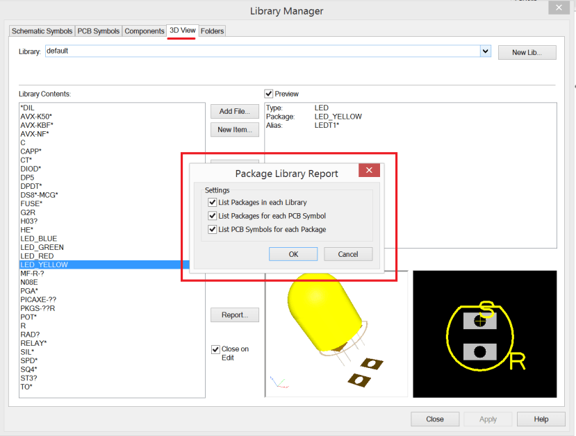
Report from the 3D page of library dialogue now has options for choices and an additional section in the report
PDF output now has the option to suppress the embedding of fonts in output file, making files much smaller
You can now choose to embed fonts when outputting a PDF file. To access the PDF Setup dialogue, go to the Output menu, Plotting & Printing, Output tab, PDF, click Device Setup and select the Embed Fonts in PDF File option.
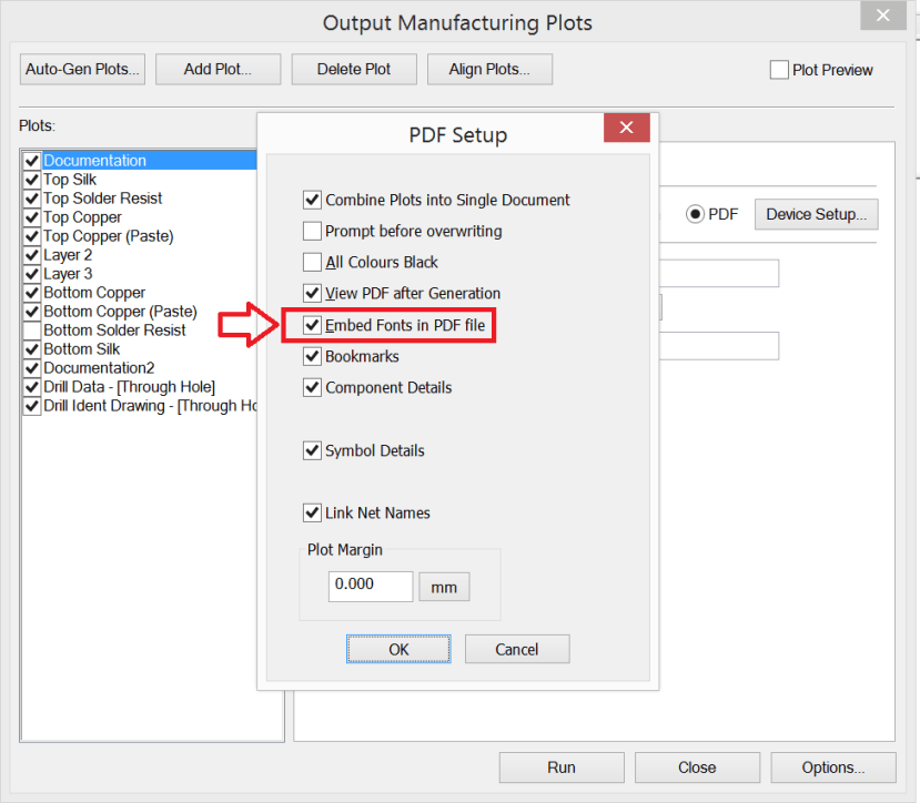
Select this option if have used true type fonts in the design and wish them to be saved into the PDF file. If this is not selected you rely on the fonts being available on other machines that the PDF file will be viewed on. The main reason that you may not want to select this is to reduce the size of the PDF file.
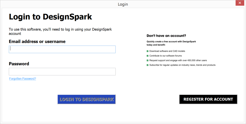
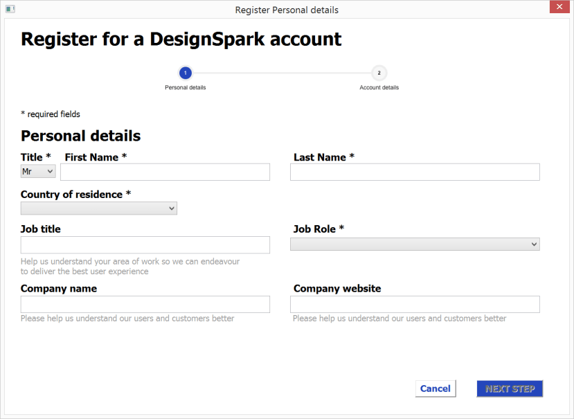
New way of logging into software and registering new users
Users have a new way of logging into the software and registering themselves as a new user. This provides an enhanced experience because they input fewer details and only have to register once for all of the DesignSpark tools. This means the user does not need to register again after installing DesignSpark PCB if she or he is already registered on the DesignSpark website.
If you haven’t tried DesignSpark PCB yet, what are you waiting for? It’s free (and always will be)