Design like a Pro - Blind and buried vias
Follow article
 Dave from DesignSpark
How do you feel about this article? Help us to provide better content for you.
Dave from DesignSpark
Thank you! Your feedback has been received.
Dave from DesignSpark
There was a problem submitting your feedback, please try again later.
Dave from DesignSpark
What do you think of this article?
For advanced PCB designs, DSPCB Engineer provides many useful enhancements. One of the features providing greater flexibility for your PCB design is the option to use blind and buried vias.
Note: to use the below feature, you will need DesignSpark PCB with an Engineer subscription.
These are simple to apply after defining the Layer Spans that are required. Vias will then use the appropriate option to connect the tracks between the layers.
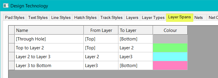
In the Design Technology select the Layer Spans tab and use Add to create the required span between the layers and select a colour.

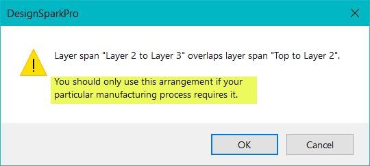
The application is totally flexible allowing any layers to be defined as "spanned" so you MUST check with your manufacturer as to what they can provide and importantly at what cost!
For this reason, an information message will occur as a reminder for you to check the span is as you require.
The layer spans are now as listed as below where you will see you can assign colours to aid your design visualisation.
Now you are all set to go!
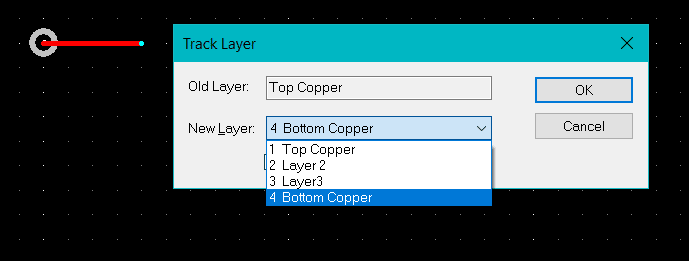
Route your tracks in your design as normal and when you change layers the normal layer options are presented, however where a layer span has been defined for the selected layer a blind or buried via will be applied.
Below shows a simple track routed to various layers and the result shown in the 3D View.
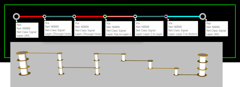
The appropriate blind or buried vias are used for layer spans where they have been defined.
If you select to route to other layers, the default "All Layers" via will be used as shown by left two vias routing Top copper to Layer 3.