Building a car battery data logger Part 2: How to measure voltages and currents in charging and discharging of car battery with STM32f407 VGT6
Follow article Dave from DesignSpark
How do you feel about this article? Help us to provide better content for you.
Dave from DesignSpark
Thank you! Your feedback has been received.
Dave from DesignSpark
There was a problem submitting your feedback, please try again later.
Dave from DesignSpark
What do you think of this article?
This part shows how to use various mode of the STM32F407 VGT6 ADCs, including:
-
Multi-channel measurement
-
DMA
An ADC (Analog-to-Digital Converter) is a peripheral that allows measuring the voltage (between 0V to Vref) on a certain input of the microcontroller and converting it into a number between 0 and 2N – 1 where N is the number of bits of the ADC resolution. Noted that in my design, Vref is connected to 3.3V and N = 12.
I will use the PC1, PC2 pins connected to channel 11 and channel 12 respectively according to STM32f407xx datasheet:

The advantage of using DMA is that we can use multi-channel conversion. The result of the conversion will be stored in the memory and at any instance during the code, we can access that memory and read ADC values within interrupt service routine.
According to the STM32F4 reference manual, ADC1 is connected to channel 0 of streams 0 and 4 of DMA2:

The ADC converted results (voltage prior to current) will be stored into ADCConvertedValue buffer that I have declared at the beginning of the code. So, index 0 and 1 associated with voltage and current information respectively in hex data representation.
To start ADC, the following needs to be done:
- Enable the ADC, DMA, GPIO clocks
- Configure the GPIO pins as analog inputs
- Configure the ADC speed (prescaler / sample time)
- Configure the DMA
- Enable continuous measurement mode
This can be done using the following code:
void ADCInit (void){ ADC_InitTypeDef ADC_InitStructure; DMA_InitTypeDef DMA_InitStructure; GPIO_InitTypeDef GPIO_InitStructure; ADC_CommonInitTypeDef ADC_CommonInitStructure;
/* Enable ADC1, DMA2 and GPIO clocks ****************************************/ RCC_AHB1PeriphClockCmd (RCC_AHB1Periph_DMA2 | RCC_AHB1Periph_GPIOC, ENABLE); RCC_APB2PeriphClockCmd (RCC_APB2Periph_ADC1, ENABLE);
/* DMA2 Stream0 channe0 configuration ****************************************/ DMA_DeInit(DMA2_Stream0); DMA_InitStructure.DMA_Channel = DMA_Channel_0; DMA_InitStructure.DMA_Memory0BaseAddr = (uint32_t)&ADCConvertedValue; DMA_InitStructure.DMA_PeripheralBaseAddr = (uint32_t)&(ADC1->DR); DMA_InitStructure.DMA_DIR = DMA_DIR_PeripheralToMemory; DMA_InitStructure.DMA_Buffersize = 2; DMA_InitStructure.DMA_PeripheralInc = DMA_PeripheralInc_Disable; DMA_InitStructure.DMA_MemoryInc = DMA_MemoryInc_Enable; DMA_InitStructure.DMA_PeripheralDataSize = DMA_PeripheralDataSize_HalfWord; DMA_InitStructure.DMA_MemoryDataSize = DMA_MemoryDataSize_HalfWord; DMA_InitStructure.DMA_Mode = DMA_Mode_Circular; DMA_InitStructure.DMA_Priority = DMA_Priority_High; DMA_InitStructure.DMA_FIFOMode = DMA_FIFOMode_Disable; DMA_InitStructure.DMA_FIFOThreshold = DMA_FIFOThreshold_HalfFull; DMA_InitStructure.DMA_MemoryBurst = DMA_MemoryBurst_Single; DMA_InitStructure.DMA_PeripheralBurst = DMA_PeripheralBurst_Single; DMA_Init(DMA2_Stream0, &DMA_InitStructure); DMA_Cmd(DMA2_Stream0, ENABLE;
/* Configure ADC1 Channe0 pin as analog input *****************************/ GPIO_InitStructure.GPIO_Pin = GPIO_Pin_1 | GPIO_Pin_2; GPIO_InitStructure.GPIO_Mode = GPIO_Mode | GPIO_Mode_AN; GPIO_InitStructure.GPIO_PuPd = GPIO_PuPd | GPIO_PuPd_NOPULL ; GPIO_Init(GPIOC, &GPIO_InitStructure);
/* ADC Common Init **********************************************************/ ADC_CommonInitStructure.ADC_Mode = ADC_Mode_Independent; ADC_CommonInitStructure.ADC_Prescaler = ADC_Prescaler_Div2; ADC_CommonInitStructure.ADC_DMAAccessMode = ADC_DMAAccessMode_Disabled; ADC_CommonInitStructure.ADC_TwoSamplingDelay = ADC_TwoSamplingDelay_5Cycles; ADC_CommonInitStructure.ADC_TwoSamplingDelay = ADC_TwoSamplingDelay_5Cycles; ADC_CommonInit(&ADC_CommonInitStructure);
/* ADC1 Init ***************************************************************/ ADC_InitStructure.ADC_Resolution = ADC_Mode_Resolution_12b; ADC_InitStructure.ADC_ScanConvMode = ENABLE; ADC_InitStructure.ADC_ContinuousConvMode = ENABLE; ADC_InitStructure.ADC_ExternalTrigConvEdge = ADC_ExternalTrigConvEdge_None; ADC_InitStructure.ADC_DataAlign = ADC_DataAlign_Right; ADC_InitStructure.ADC_NbrOfConversion = 2; ADC_Init(ADC1, &ADC_InitStructure);
/* ADC1 regular channel configuration *****************************************/ ADC_RegularChannelConfig(ADC1, ADC_Channel_11, 1, ADC_SampleTime_15Cycles); ADC_RegularChannelConfig(ADC1, ADC_Channel_12, 2, ADC_SampleTime_15Cycles);
/* Enable DMA request after last transfer (Single-ADC mode) */ ADC_DMARequestAfterLastTransferCmd(ADC1, ENABLE);
/* Enable ADC1 DMA */ ADC_DMACmd(ADC1, ENABLE);
/* Enable ADC1 */ ADC_Cmd(ADC1, ENABLE);
ADC_SoftwareStartConv(ADC1);
Idea of calculation
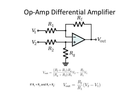
To convert the ADC value (from 0 to 0xFFF) to a voltage or current value (from 0 mV/mA to 3.3 mV/mA), each element of ADCConvertedValue buffer have to multiply by 3300 and divided by 0xFFF. As a result, I have got the voltage of Pin PC1 and PC2. As mentioned in part 1, PC1 and PC2 actually are the output terminals for two different differential op amp. So, I am able to find the values of Vbattery and VI_SEN by the relationship between Vin and Vout of an op-amp differential amplifier shown below. However, the current sensing part have been stepped up, so ADCConvertedValue [1] have to minus 1650 before passing into op-amp calculation to see whether the current is neither positive or negative (charging or discharging). Then, referring to the datasheet of current sensor has 100-s to calculate back the original current value.
In next part, I will talk about how to apply timer interrupt to get ADC converted result and then to transmit these data to my PC through Wi-Fi module. Afterwards, we can create a php file to listen to the incoming sockets from a port and then put them into my MySQL database so as to plot a line chart on a webpage.