How Can I Pour Copper in DesignSpark PCB?
Follow article
 Dave from DesignSpark
How do you feel about this article? Help us to provide better content for you.
Dave from DesignSpark
Thank you! Your feedback has been received.
Dave from DesignSpark
There was a problem submitting your feedback, please try again later.
Dave from DesignSpark
What do you think of this article?
Copper Pour is used to flood areas of a PCB layout with copper, usually connected to a nominated signal through ‘thermal’ connections, typically Ground (0V) or +5V. This facility will then create voids around tracks, component pads, vias and other electrical obstacles.
For this, we have the Add Copper Pour Area and Pour Copper options.
If a copper area is to be inserted without the need for voids around unconnected tracks, components or pads, the Add Copper option can be used.
The principle of this facility is to insert a Copper Pour Area and ‘pour’ the copper into this area.
Creating a Copper Pour Area
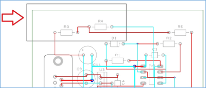
From the Add menu, select Copper Pour Area > then Rectangle. Other Pour Area options are available for adding different shapes. In our example below, we will add the pour area to the Top Copper layer. Pour areas and poured copper can be added to any electrical layer. To change layers, select the pour area and click <L> followed by <Enter> as we did when editing tracks.
The shape can be created on the design and the pour area can be drawn protruding outside the board outline. DesignSpark PCB will pour the copper using the Spacing rules and rules defined for the Pour area.
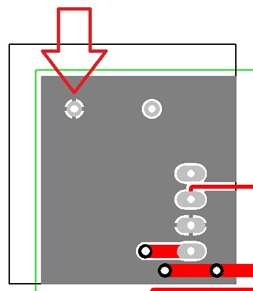
Following our example below, draw a basic rectangle pour area shape, this is shown in black on the top left-hand side of the design:
For this example, you will see how easy it is to add a poured copper area.
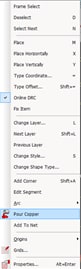
Right-click on the pour area.
From the shortcut menu select Pour Copper.
A dialogue box is displayed from where you can select parameters for the poured area, such as the net name association and thermal connections etc.
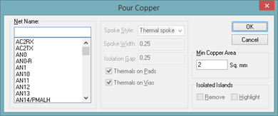
For this exercise, leave the Net Name blank and simply click OK.
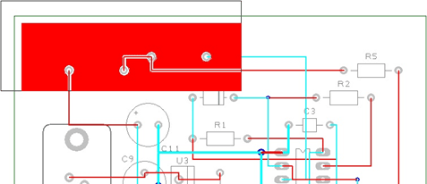
Notice that the poured copper has obeyed the Spacing rules of all defined items to copper including Board to Shape rules.
Making the Copper Pour Area intelligent
There are more facets to the poured copper than we have discussed above. The poured copper can also have a net name associated with it so that when poured, pads are connected via thermal spokes to the copper itself. To do this, select the pour area and from the shortcut menu select Add To Net. Select the net name required from the list and then re-pour the copper. Try it again using GND as the net name and click OK.
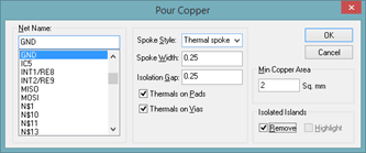
Using the Spoke Style checkbox settings for Spoke Style, Spoke Width and Isolation Gap, the style of how the copper is connected to pads can be defined.
In Spoke Style: type Spoke 10. Type 10 for Spoke Width: and 10 for the Isolation Gap, then press OK. When requested, add the new style, Spoke 10 to the Technology.
The Copper Pour Area line will not appear on your manufactured boards, they provide the system with an intelligent area into which the copper can be poured.
You’ve added it, so how do you take it away?
To remove a poured copper area (including any thermal spokes), simply select the area outline and select Clear Copper from the shortcut menu. This removes the copper but not the Copper Pour area.
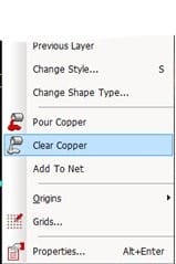
When using poured copper remember that you shouldn’t use Delete but should always use Clear Copper. Copper Pour Areas can be modified at any time and the area re-poured using the option from the shortcut menu. If you wish to completely remove the copper and area, you must use Clear Copper first and then delete the area afterwards using the Delete key.
For more hints and tips on how to use DesignSpark PCB you won’t go far wrong taking a look in our Zendesk support area.
See the original article here
If you still haven’t downloaded DesignSpark PCB, what are you waiting for?