Quick Start Guide to DSPCB.
Follow article
 Dave from DesignSpark
How do you feel about this article? Help us to provide better content for you.
Dave from DesignSpark
Thank you! Your feedback has been received.
Dave from DesignSpark
There was a problem submitting your feedback, please try again later.
Dave from DesignSpark
What do you think of this article?
Quick Start Guide to DSPCB.
Having downloaded DSPCB and activated it the following is a quick guide to getting your schematic and PCB layouts created and ready for manufacture.
DSPCB has Wizards available to assist you through each step, which in many instances is a simple selection process making this easy and intuitive.
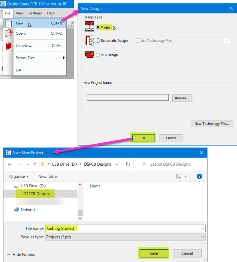
Create a Project.
The first step is to create a "Project" which will contain the schematic and PCB designs.
File - New
Select "Project" - <OK>
Save the New Project in its own folder to keep all the project files together.
DesignSpark PCB now has a new tab for the created project.

Add a schematic sheet.
Next, add a schematic design sheet to the Project.
File - New.
Select "Schematic Design"
Tick "Use Technology File" and select a Technology file from the pull-down list, Default (white) is recommended.
Ensure "Add to Open Project" is also ticked and click <OK>
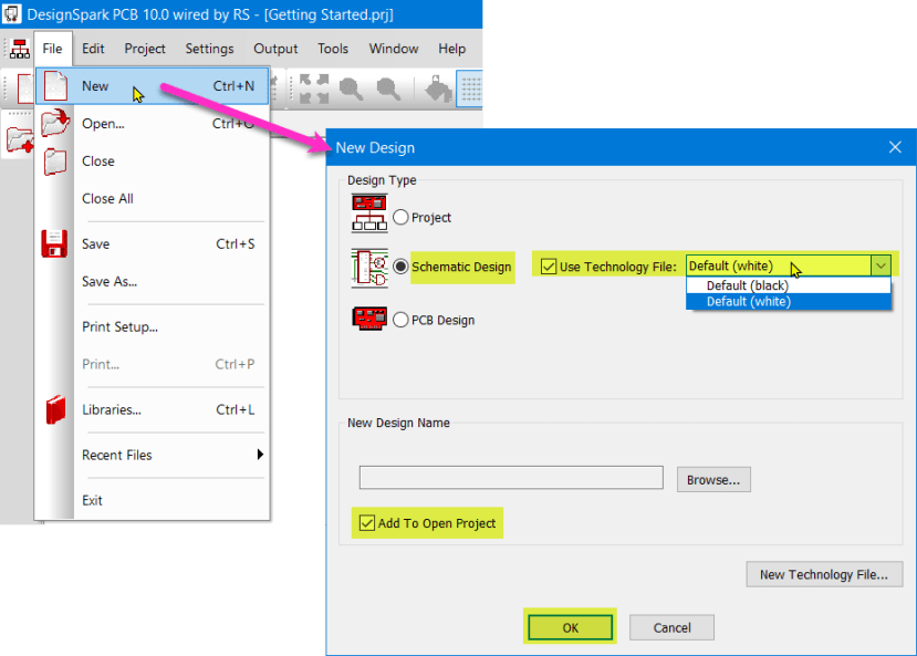
In the window that opens, name the schematic sheet as you wish and click <Save> to add it to the Project.

A new tab will be created for the schematic sheet which will also be listed under the project tab.
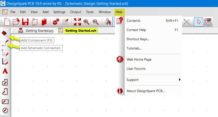
Below shows the essential minimum details to start your design.
Add Component accesses your libraries from where you can select and load components onto the schematic sheet.
Add Schematic Connection allows you to interconnect the components to complete your design.
Help options are available from the menu bar, which as well as the Help file includes useful links for quick access to the online resources and a handy document on the allocated Shortcut Keys.
Congratulations you can now complete your schematic design with these minimal features. DSPCB offers far more than the above which you can explore later as described at the end of this article.
At this point, it should be mentioned that your libraries are relatively empty! This is to allow you to build up your own custom and efficient library without having a huge cumbersome library of parts you may never use installed.
How to build up your User library is described in the following links which provide you with access to a huge online resource to select from.
Create your PCB.
Using the example schematic below we illustrate the steps to produce a printed circuit board.
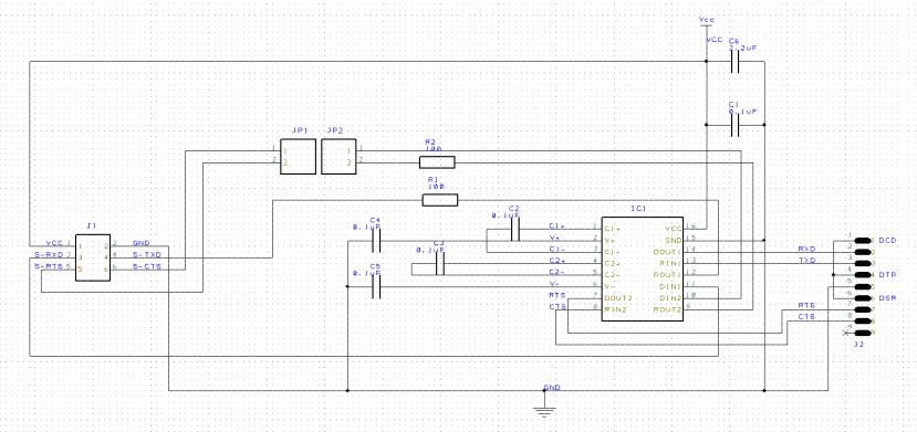
A "Wizard" guides you through the essential steps, each step requires just a few simple selections and a click on <Next> to get to the next step as shown below.
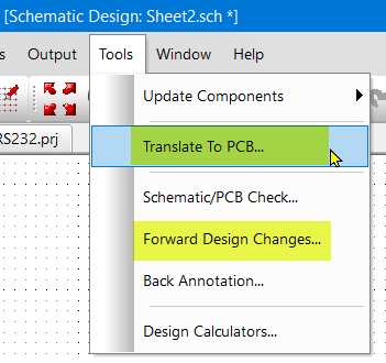
From the "Tools" menu select "Translate to PCB..." the first time you create your PCB.
Should you make subsequent changes later in the design process then you will use "Forward Design Changes..." as you already have a PCB with components and only require the 'changes' to be forwarded.
.
The Wizard now starts with the introductory window, click <Next>..

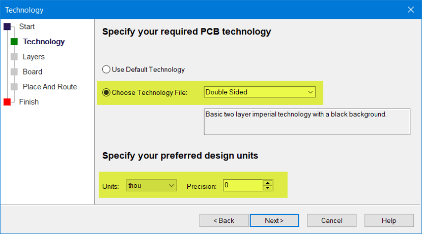
Here we select the Technology File. This is an important step as it preloads a typical set or parameter used for the layout. You do not need to worry about these at the moment and a useable PCB design will be created.
We recommend selecting "Double Sided" to start with to gain familiarity with the process. This is useful for single sided as well, just place the required copper tracks on the bottom side. You can place copper tracks on the top side to simulate link wires and provide connectivity for checking purposes.
You can also select your preferred units and the "precision" which is the number of digits after the decimal point. It is important to note that this is for "display purposes" only as everything is done internally with maximum precision within DSPCB.
Here just select "Use Layers From Chosen Technology File" and click <Next>.
All the required layers will be produced by the program even if you do not select them at this point.

Now you select a board size, however, this is easy to change in the PCB design steps so just click <Next>.

For component placement select "Arrange Outside the Board". This will allow you to select each component and place it in a logical position on the board. Just click <Next>.

Finally provide a name for the PCB and it will be saved in the Project folder. Click <Finish> to start your layout process.

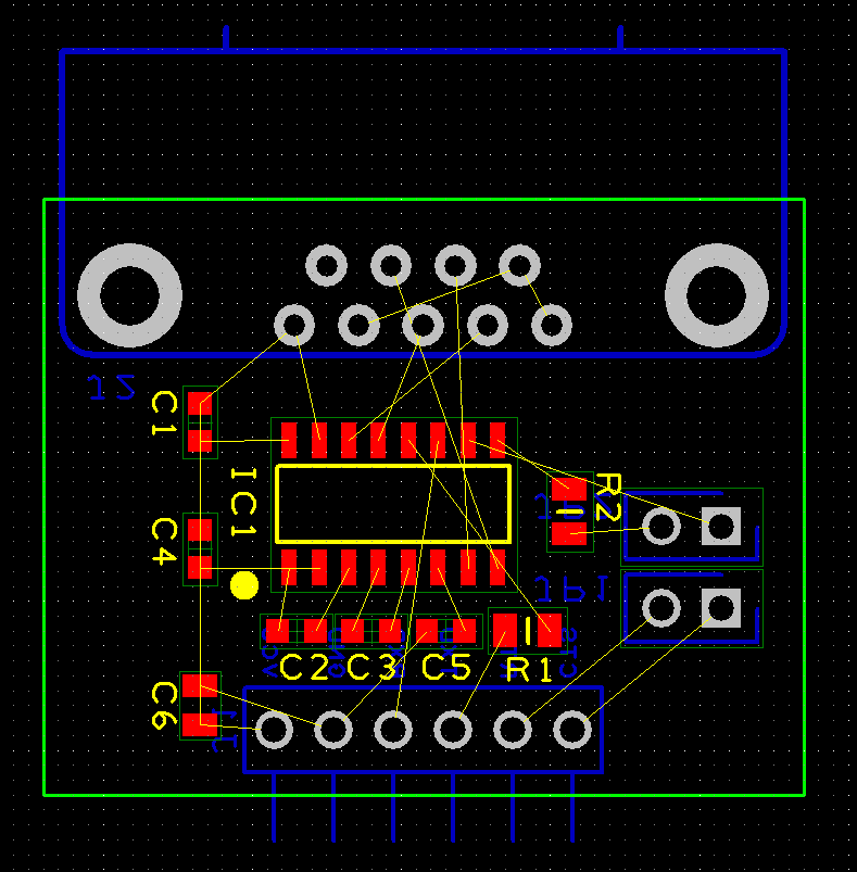
Using our example schematic you will see something like that shown below.
The components are outside of the board area (green box) and each pad is shown with a net connection line known as an "air wire" or "rubber band" and the view is commonly referred to as a "rats nest".
Your task is now to select each component and position it on the board and route a copper trace in place of each rubber band connection.

To select a component use Shift + LMB (left mouse button) when the mouse is over part of the required component, this will select the complete component and any text.
Move the component to the desired location and click to place.
To change the orientation, with the component selected use the shortcut "R" to Rotate 90 degrees and repeat as required.
Note for when you get more advanced, shortcut "F" will Flip the component to the other side of the board.
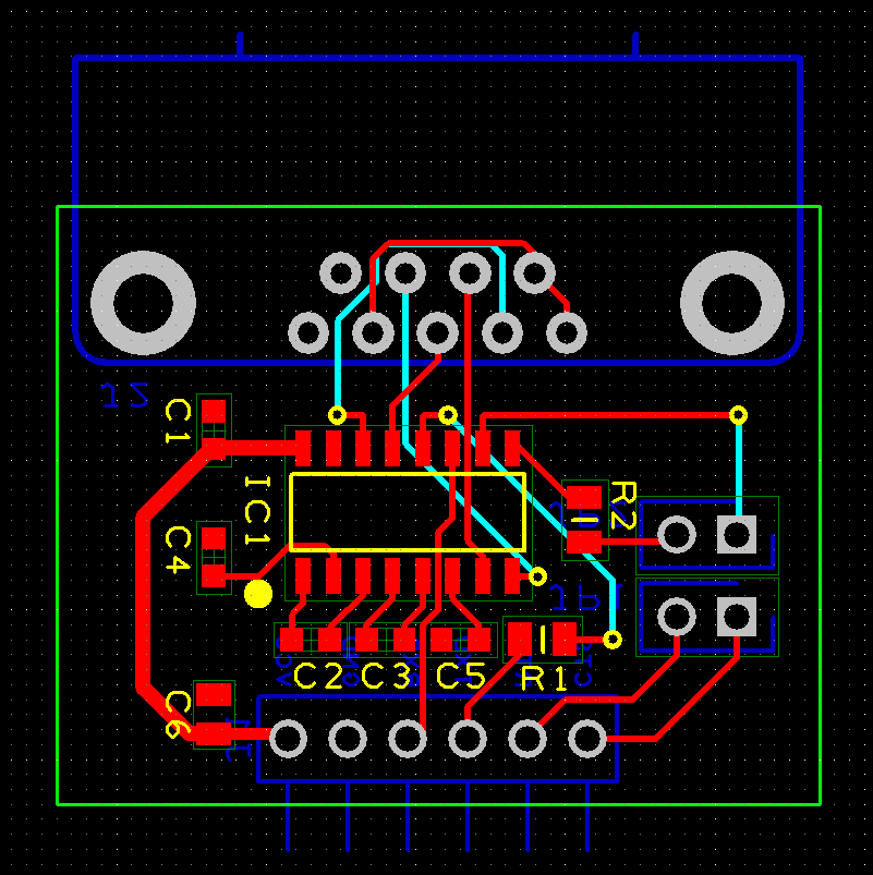
Here is our example with the components positioned and orientated showing the air wires that require to be routed.
Tracks are placed by a double click on the air wire and routed as required. Click to place the track when you wish to change direction.
Below is our example board when finished routing.
Manufacturing your PCB.
Now you have your PCB layout you will wish to get it manufactured.
DSPCB provides the option to produce Gerber plots that you can submit to any manufacturer.
How to produce Gerber plot files.
Alternatively to produce PDF plots for your own use.
How to produce PDF artwork plots.
For further details on both techniques please review the other articles in Output documents.
BEFORE you create any of the above there are tools to check your design.
The DRC (Design Rules Check) will check the basics of your design such as track widths, spacing, silkscreen text overlaps and much more.
How can I check my PCB layout.
This guide provides further details of what can be checked to ensure you produce what you intended to design.
There is much more available to help you be creative and productive as your design experience and requirements grow.
In addition to the "Help" file, there are online resources to assist you.
DesignSpark PCB Tutorials, Guides, Videos and articles
and also DesignSpark PCB Articles here.
Have fun being creative!