Eurocircuits - Using a Design Technology file for minimum costs.
Follow article
 Dave from DesignSpark
How do you feel about this article? Help us to provide better content for you.
Dave from DesignSpark
Thank you! Your feedback has been received.
Dave from DesignSpark
There was a problem submitting your feedback, please try again later.
Dave from DesignSpark
What do you think of this article?
The partnership between DesignSpark and Eurocircuits provides the opportunity for both PCB and assembly for prototypes through to production runs. The opportunities are discussed by Greig and Pete Wood from DesignSparks and Dirk Stans from Eurocircuits in this article.
Let's explore using DSPCB for a minimum cost board manufacture, but first, have a look at RS/DesignSpark partnership with Eurocircuits page. Here you will find some links to interesting videos of the factory and the processes along with the tools available for checking prior to any manufacturing.
For DSPCB the settings in the Design Technology files should be set to ensure you keep to the basic cost options where possible this ensures you do not design a more expensive PCB than necessary. Basically, this entails using tracks and spacing along with pads and holes that do not encroach into the premium and specialist production areas.
The good news is that the Design Technology file "Double sided (metric).ptf" file is usable straight away!
Here we continue our discussions on what Eurocircuits offers and how you can create a custom design technology if required.
Eurocircuits provide a PCB Configurator which will analyse your Gerber plots and determine the Technology Class that your PCB requires and will determine the final price.
Note. You will see that each of the above two web pages has many links to other information to assist you. Also, click on the images to get a larger view.
Looking at the "Classification" you will see what settings to use in your Design Technology to meet the lower-cost manufacturing.
We now examine the requirements for a Prototype or Standard Pool PCB manufacture for a double-sided PCB.
If you have different requirements you can explore the other options or design your PCB as you require and use the PCB Configurator for a report on your design.
The Prototype and the Standard Pool services have the following requirements.
Highlighted is the minimum class which we shall use in our Design Technology.
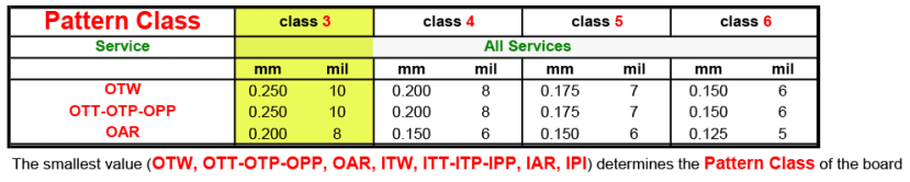
Figure 1.
The pattern class covers the minimum sizes for copper track (conductor) and gap (isolation) for Outer layers:
NOTE, the abbreviations are preceded by "O" to define outer layers and we have extracted only that data for this example.
Outer layer
- OTT = Track to Track
- OTP = Track to Pad
- OPP = Pad to Pad
- OTW = Track Width
The minimum copper rings on the outer layer.
- OAR = Outer Annular Ring
Copper to the board edge on the outer layers is also specified as 0.25mm minimum. There are exceptions to this for special applications as discussed here.
There are similar requirements for drilled hole sizes.
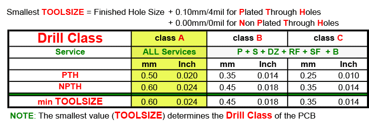
Figure 2.
We will use these in our Design Technology file and use the following minimum values:
Track to track, track to pad, pad to pad and track width are required to be 0.25mm (10 mil) minimum.
We also assume copper shape to any other copper is 0.25mm.
Any copper to the board edge is specified as a minimum of 0.25mm (10 mil) however in most cases you will set this at a greater value. Full details of how Eurocircuits handle any boards where your design has less than the specified 0.25mm spacing or if you require copper up to the board edge are detailed here.
In DSPCB, you can open a PCB Technology File to view, edit and save the file.
Opening the double sided (metric).ptf file which is in your public folders for DesignSpark PCB, use the shortcut key Shift+T and select the "Spacings" Tab.
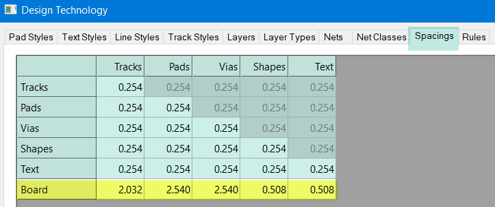
Figure 3.
As can be seen, everything is set as required plus you have some leeway if you need to reduce the distances closer to the board edge.
Next, examine the "Track Styles".
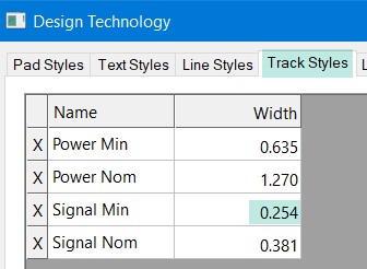
Figure 4.
Again the minimum track style used is for Signal Minimum and is set as required.
Now examine the "Pad Styles".
This is slightly more complicated, Eurocircuits specify a minimum tool size of 0.6mm however the Design Technology specifies the final hole size after plating. The good news is that Eurocircuits calculate the required drill size to allow for plating, so all drill sizes will be larger than the listed 'hole sizes' specified in the Design Technology for a through plated hole.
(Note if you were designing a single-sided PCB then the hole size listed should be a minimum of 0.6mm)
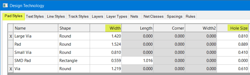
Figure 5.
Examining our list of Hole Sizes for pads, with the exception of the "Small Via" all are greater than 0.6mm.
Eurocircuits however specify the requirements of vias differently from pads as they have a lower tolerance on the final hole size as they do not have a component lead inserted.
Any hole smaller than 0.45mm is considered a via.
For the standard pool service, The minimum requirements on the via elements are:
Minimum annular ring 0.1mm
Minimum Hole size 0.1mm
The minimum pad size (for 0.1mm via for 0.1mm annular ring) is 0.4mm
The provided "Design Technology" exceed all the minimum drill size requirements.
If you wish to have a better understanding of drilled holes and how the drill size is selected this Eurocircuits page provides further details.
We now need to consider the required minimum pad widths
In figure 1, a value of 0.2mm is specified for "OAR" which is the width of the "Outer Annular Ring" and is defined as below.
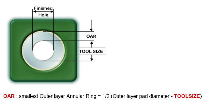
Figure 6.
Our design technology specifies the final hole size, not the tool size. How do we handle this regarding the pad size?
Eurocircuits state:
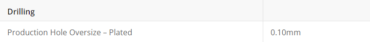
For all through plated holes, the Tool Size is the Hole Size (see Fig 5) plus 0.1mm.
Therefore the pad size diameter (Width in Fig 5) must be equal to or larger than:
Pad size = Hole Size + 0.1mm oversize + 2 x (0.2mm) OAR i.e. Pad size is the Hole Size + 0.5mm (or larger).
Again we are fortunate that all the pad widths in our Design Technology (Fig 5.) are greater than this minimum.
Conclusion.
Using the supplied Double Sided (Metric) pcb technology file will allow you to design a minimum cost PCB.
You will shift to higher cost board manufacture if you use smaller custom tracks, these may be required for some surface mount components, but using the Eurocircuits Configurator will allow you to visualise where these costs have been incurred.
Check out Eurocircuits for your next design.