Dual-Core microcontrollers: RP2040 v dsPIC33CH
Follow article
 Dave from DesignSpark
How do you feel about this article? Help us to provide better content for you.
Dave from DesignSpark
Thank you! Your feedback has been received.
Dave from DesignSpark
There was a problem submitting your feedback, please try again later.
Dave from DesignSpark
What do you think of this article?
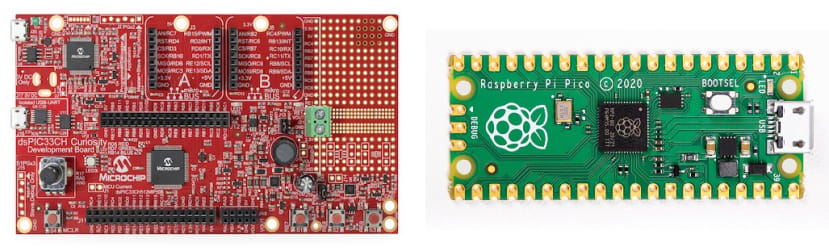
Left: Curiosity development board for dsPIC33CH. Right: Pico development board for RP2040.
Multicore microprocessors are de rigueur in any ‘high-performance’ computer now, but what about the humble microcontroller? Two such devices have come on the market recently: the Raspberry Pi RP2040 and the Microchip dsPIC33CH, both with two cores.
Microchip dsPIC33CH
The dsPIC Digital Signal Controller has been around for many years, getting faster with more bells and whistles added with each new generation. Basically, it’s a PIC24 16-bit microcontroller with extra digital signal processing (DSP) hardware and an extended instruction set. The CH variant is essentially two complete single-core dsPIC33 processors on one die, plus some inter-core communication channel hardware.
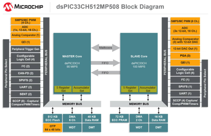
This simplified block diagram shows the specific features of the dsPIC33CH512MP508 device supplied with the Curiosity development board (187-6209) . It’s immediately apparent that the processors are not identical. The cores themselves are probably the same; it’s all the paraphernalia around them such as memory and peripherals that’s different:
- The Master has more program/data memory, and the Slave’s program memory is volatile RAM, not Flash. The Master also has more communication channels, including SENT (Single-Edge Nibble Transmission: ideal for automotive applications apparently).
- But the Slave is faster; 100MIPS next to the Master’s 90MIPS. It also has the lion’s share of peripheral devices such as ADCs and a DAC.
On power-up, the Master runs the code in its Flash program memory and if no reference is made to the Slave, operation continues as if it were a single-core device. Any program code for the Slave is kept in a special area of the Master’s Flash memory and is automatically transferred after a Power-On-Reset to the former’s program RAM (PRAM) where it will run.
DSP features
One problem the dsPIC always had was that the normal working registers were ‘repurposed’ when some DSP instructions such as multiply-accumulate (MAC) were executed. This meant a lot of overhead, saving and afterwards restoring the affected register contents. With the ‘Cx’ part (CH is dual-core, CK is single core) all working registers and the two 40-bit DSP accumulators are ‘shadowed’ allowing for very fast context switching with little time penalty. Having a second core available offers the prospect of the Slave acting as a co-processor to the Master, executing DSP-intensive algorithms, such as an FFT, at 100MIPS. I suspect this is why the Slave has control over most of the ADC input and PWM output functions.
Safety features
It’s obvious from looking at all the features dedicated to functional safety that this dsPIC is aimed firmly at applications requiring a high degree of immunity from failure.
- Program memory contents protected by Error Correcting Code (ECC).
- Built-In Self-Test (BIST) circuit checks out data RAM after power-up reset.
- 32-Bit Programmable Cyclic Redundancy Check (CRC) engine for communication channel integrity.
- On-board Watchdog (WDT) and Deadman (DMT) timers.
- Slave can be used as a redundant check processor as part of an ISO26262-compliant fault-tolerant system.
- Chips tested to AEC-Q100 quality standard.
- Wide operating temperature range: -40 to +125°C
Clearly, Microchip have automated industrial and automotive ADAS applications in mind for the dsPIC33CH device.
Development tools
The Curiosity board comes with a programming/debug interface (PKOB) already fitted. Plug in a USB cable connecting the board to a PC running Microchip’s MBLAB X IDE and you’re done. You can now program and debug the Master or Slave code – just not at the same time. To watch both cores running at the same time a second debug tool is needed. Populate the ICSP ‘Slave Debug Only’ pads with a 6-pin header and plug in a PICkit 4 or ICD 4. A second USB cable connection is made to the PC, whereupon a few mouse clicks will make the activity of both cores visible in the IDE window.
The board is supplied fitted with some useful extras. If you’re developing a switch-mode power supply (SMPSU) then there are a number of components to assist you. Personally, the items of greatest interest are the two MikroBUS sockets and the isolated USB socket with a UART bridge chip. I plan to port FORTHdsPIC across from the MikroElektronika Clicker 2 board currently hosting it, and the Click peripheral modules I’ve accumulated can come too!
Raspberry Pi RP2040
After years of shoe-horning ever more powerful ARM processor cores into successive generations of chips on Single-Board Computers (SBC), the good folks at Raspberry Pi decided to design a microcontroller chip from scratch. For the first time, developers and manufacturers are able to buy RPi chips in quantity to incorporate in their own board designs. Fortunately for everyone else, the RP2040 is also available on a development board called Pico. The association with ARM continues however, as the core used is the Cortex-M0+, a popular choice for small low-power embedded devices.
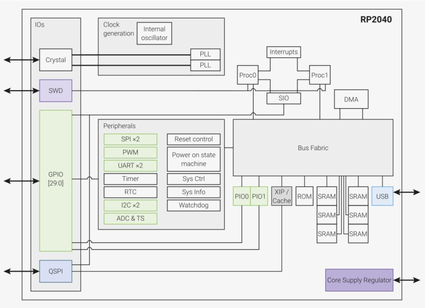
Looks completely different from the dsPIC doesn’t it? In fact, it’s easy to miss the two processor cores, Proc0 and Proc1 located top right. The twin-core system is described as symmetrical and as such is nothing like the dsPIC’s dual-processor arrangement. Both cores activate on power-up and read the status of their respective CPUID registers. Proc0 will see a ‘0’ and begin executing code while Proc1 will see a ‘1’ and go back to sleep. As with the dsPIC, the second core does nothing after reset until activated.
One set of peripherals is shared between the cores via a programmable crossbar bus system. They even share the same external Flash memory chip via a QSPI bus. There is no intrinsic Master-Slave relationship here; either core can access all resources. But the cost of this democracy is ARM’s ultra-fast and complex Advanced High-Performance Bus (AHB) bus structure linking everything together. Fortunately for the programmer, this is all largely invisible, but covered in detail in Chapter 2 of the RP2040 datasheet if you’re interested. All this bus sophistication brings with it an economy in silicon because almost all duplication of resources (redundancy) is eliminated. The designer can also tailor the amount of Flash memory available to suit the application up to a maximum of 16MB.
The big feature of the RP2040 that’s excited the most interest is the block of eight PIO pins, each driven by a programmable state-machine. The state-machine is like a very simple processor core and will allow, for instance, complex serial communication protocols to be used without bothering the main processors.
The Boot ROM
Take a close look at the block diagram and you will find a tiny box marked ‘ROM’. It’s strange that the headline feature list for the device makes no mention of it. Turn to page 156 of the RP2040 datasheet and you will find an inventory of that ROM. It’s a goldmine of useful goodies:
- Core 0 initial start-up sequence.
- Core 1 low-power wait and launch protocol.
- USB MSC class-compliant bootloader with UF2 support for downloading code/data to Flash or RAM.
- USB PICOBOOT bootloader interface for advanced management.
- Routines for programming the external Flash memory.
- Fast IEEE-754 SP and DP floating-point maths library.
- Fast bit-counting / manipulation functions.
- Fast memory fill / copy functions.
The key item is the bootloader – it’s located in the chip itself, so works regardless of the target board design. The floating-point library is a real bonus, but remember these are optimised software routines and will not have the speed of the hardware floating-point unit that comes with the Cortex-M4F cores.
Development tools
The Pico (212-2162) is about as basic a development board as you can get: the RP2040 chip, power supply regulator, 2MB Flash memory, a few ‘discretes’, and that’s it. However, unlike the dsPIC Curiosity board, it is designed to be built into a target system. It does have the means to activate the on-chip ‘bootloader’ described above: holding down the BOOTSEL button while powering up makes it appear as a folder to a USB-connected PC. Program files in .uf2 format can just be ‘dragged-and-dropped’ onto this Pico folder. The bootloader will blow them into Flash memory and run them. No debug features are available and this method is really only useful for an initial checkout with a ‘Hello World’ program. For real development, you need to use ARM’s 3-wire SWD programming interface that’s brought out to header pads on the opposite end of the board to the USB connector. The problem is you can’t just plug them straight into a PC. Like the dsPIC, a programming/debug interface is needed. Raspberry PI don’t provide anything like the PICkit or ICD, but two options are available:
- Connect the SWD pins to GPIO pins of a Pi 4. Undoubtedly this is the best method as the Pi is easily set up to work up with the Pico board.
- If you really must use a desktop machine for development, then a second Pico can be programmed to provide the hardware interface.
Raspberry Pi should really think about providing a debug tool boxed-up like the Microchip PICkit.
UPDATE: Raspberry Pi have released just such a debug tool.

RP2040 v dsPIC33CH
Really, about the only thing these two devices/boards have in common is that each has a dual-core processor! They are aimed at widely different markets though:
RP2040
Being incredibly cheap and compatible with the Pi 4 for development, the Pico board is great for experimenters and Makers. By making the chip (221-1609) available in bulk quantities suggests that Raspberry Pi want a slice of the OEM market. Although the .uf2 bootloader is useful for beginners to check that their new Pico board works, I think its main purpose is to make production programming easier. The specified operating temperature range of -20 to +85°C exceeds that recommended for commercial applications, but falls a bit short of industrial. The first RPi microcontroller chip seems best suited for low-power, undemanding IoT applications - perhaps a future model might see at least one of the M0+ cores replaced by an M4 to take advantage of its massively enlarged instruction set with DSP support. Artificial Intelligence based on TinyML is then a real possibility.
dsPIC33CH
The dsPIC33 has come a long way since the first version appeared many years ago. It’s clear that Microchip have designed the ‘C’ version for industrial control in harsh environments where faults can have fatal consequences. More of a carthorse than a racehorse, it’s not built for speed, but reliability, and with its large range of communication channels and on-board peripherals, versatility too.
If you're stuck for something to do, follow my posts on Twitter. I link to interesting articles on new electronics and related technologies, retweeting posts I spot about robots, space exploration and other issues. To see my back catalogue of recent DesignSpark blog posts type “billsblog” into the Search box above.