What engineers need to know about graphene
Follow article
 Dave from DesignSpark
How do you feel about this article? Help us to provide better content for you.
Dave from DesignSpark
Thank you! Your feedback has been received.
Dave from DesignSpark
There was a problem submitting your feedback, please try again later.
Dave from DesignSpark
What do you think of this article?
Graphene - the super material that will define future tech
Comprising a single layer of carbon atoms held together by super-strong nuclear bonds, graphene is a material that has numerous remarkable characteristics that are certain to prove hugely beneficial to many facets of our society. From an electronics perspective, its electron mobility, optical transparency and incredible durability are all highly attractive traits. Here, we give a brief overview of how, in the near future, certain key attributes associated with graphene could be leveraged by electronics engineers in order to accomplish new feats in terms of performance and functionality.
The graphene backstory
Graphene was initially theorised about as far back as the late 1940s. Over the decades that followed, though attempts were made to isolate the material, these unfortunately failed. Then, in 2004 two academics at the University of Manchester (Professors Andre Geim and Kostya Novoselov) succeeded in being the first to isolate a graphene monolayer. Exfoliating it from a sample of bulk graphite, they thus were able to create a material that only exists in two dimensions (2D). Geim and Novoselov later received the Nobel Prize for Physics for their efforts.
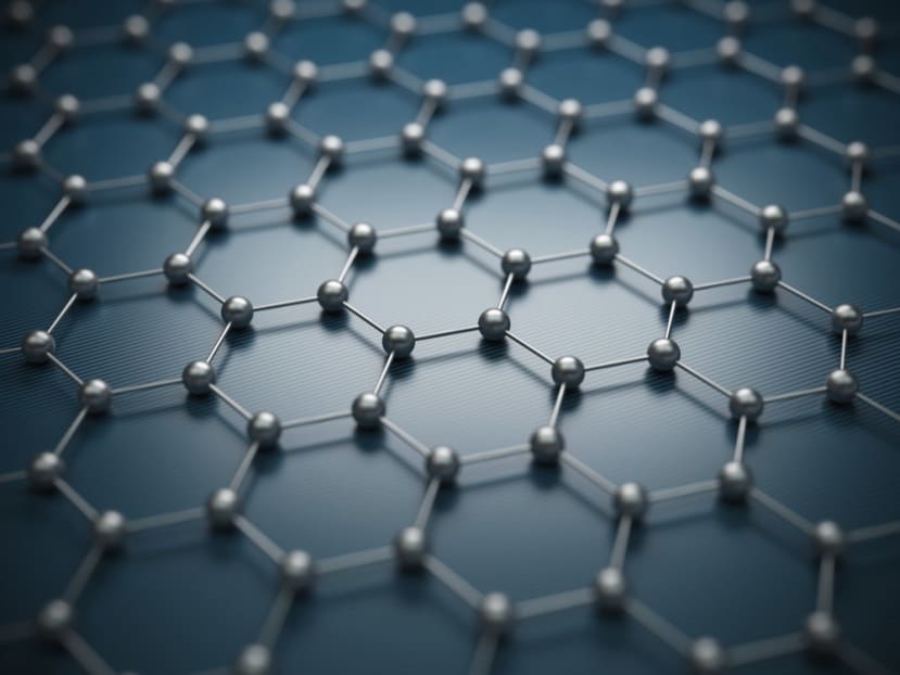
Figure 1: Illustration of a graphene monolayer
Within graphene’s distinctive honeycomb structure, the layer of carbon atoms measures just 0.34nm in thickness. Consequently, this ultra-thin nanomaterial exhibits very high degrees of flexibility. Each carbon atom in the honeycomb is bonded to three neighbouring carbon atoms - and it is this that gives the material its exceptional strength; something that it shares with other carbon allotropes like diamond. The bonding arrangement means that three out of the four outer shell electrons that each carbon atom has are used for bonded purposes. In other carbon-based materials, the fourth electron would normally take care of bonding to other planes, but since graphene is a 2D material it is no longer needed in that respect.
So, what happens to the fourth electron? The spare electrons from all the carbon atoms in the graphene lattice are delocalised - which is why graphene has strikingly higher levels of electron mobility. Figures of 35,000cm2V −1s−1 are achievable, which are far above the 1,000cm2V−1s−1 normally witnessed in silicon, or the 4,000cm2V−1s−1 of gallium arsenide. The upshot of this electron mobility is that graphene can be considered as a zero-bandgap material, offering unmatched thermal and electrical conductivity.
Graphene in electronics
As already discussed, thanks to its structure graphene possesses some unique properties. Many of these are of particular relevance in an electronics context.
The use of graphene-based transistors would mean that the validity of Moore’s Law could be prolonged a lot further. The much smaller transistor channel dimensions that these could support (compared to conventional silicon transistors), alongside the aforementioned electron mobility, would translate into switching speeds that are acutely accelerated. Microprocessors capable of running at dramatically elevated frequencies and which are more compact could thus, in principle, be developed.
Currently, touch screen displays generally rely upon the deposition of indium tin oxide (ITO) onto their outer surfaces. This transparent and conductive material enables touch points to be determined. It should be noted though that ITO is hampered by the scarcity of indium resources - with this substance featuring on the European Union’s list of critical raw materials. ITO is brittle, making it inapplicable for modern flexible electronics implementation. As ITO is a pollutant, its environmental impact also needs to be taken into account. Substituting ITO with graphene would mean that displays could benefit from heightened conductivity and transparency. It would also allow touch-enabled displays that are bendable to be produced. Likewise, graphene has the ability to boost photovoltaic performance, so that greater energy conversion efficiencies may be achieved. Extensive trials are currently being carried out on graphene-doped perovskite solar cells. These have already been able to reach conversion efficiencies of above 26%.
Supplementing emerging semiconductor technologies, like silicon-carbide (SiC) and gallium-nitride (GaN), graphene is expected to be of considerable value to power electronics too. Through it, improvements to the functionality of next generation power discretes (such as MOSFETs and IGBTs) will be feasible, since graphene is capable of dealing with even the most extreme of operating conditions. Inclusion of graphene in the electrodes of batteries will lead to faster charge times and also allow a greater number of charge cycles to be supported.
In terms of thermal management within electronic systems, graphene is once again a very attractive proposition. With a figure of around 4000-5000W/mK, it has a thermal conductivity that is more than an order of magnitude greater than copper. Generated heat energy can therefore be dissipated more effectively, meaning that the board space allocated to heatsinking mechanisms will be substantially less. This will be highly advantageous in applications where electronic hardware is densely packed together, such as in data centres. Finally, the inherent flexibility of graphene is certain to give this nanomaterial considerable traction within the wearable electronics market; for instance in smart dressings and patient monitoring systems.
Though there is the prospect of revolutionising a plethora of different areas of electronics engineering via use of graphene, major technical challenges still need to be overcome. Composites and coatings may be able to gain notable advantages by employing poorer quality, multi-layer graphene - which is already relatively easy to fabricate. However, for real value to be derived within the electronics sector, it will be necessary to produce high-quality single-layer graphene. Though this is possible in small quantities within research labs, doing it in large volumes is still proving very difficult. This has held graphene back, preventing it from moving out of the theoretic world and into a commercial reality. The volume processes that currently exist generally employ some form of chemical vapour deposition. This is far from ideal though, as after fabrication the graphene has to then be transferred onto the semiconductor substrate - with contamination and structural issues resulting. Better methods must be found for fabricating graphene at scale. This is true not just for electronics, but for a wide range of industry use cases. To add further complexity to this, with specific relevance to the semiconductor industry, it will be essential that any process conceived is able to accommodate the back end of line (BEOL) activities that go on after the graphene elements have been added - so that the addition of other features (like passives) won’t damage the graphene.
There are currently numerous different research organisations and private companies trying to develop effective methods to scale up graphene fabrication while still assuring the quality of the end product. The hope is that these will allow the issues that current processes bring with them to be avoided. With its financial backing coming directly from the European Commission, the Graphene Flagship is going to play a major role in the progression of graphene technology. Bringing together leading academic institutes and industrial partners, it provides support to key research projects with the objective of accelerating their commercialisation. The work it is currently involved in spans across a wide variety of industry verticals.

Figure 2: The ground-breaking flash graphene process [Courtesy of Rice University]
There are various routes to large volume graphene fabrication that are currently being investigated. One of those which is gaining a lot of attention right now is flash graphene. Here waste products with high carbon content are exposed to ultra-high heat levels (over 3000K) for a very short period (under 10ms). This ‘flash’ of heat causes all the carbon atoms bonds to break, then the rapid cooling that follows sees them form into separate graphene monolayers. A further plus point is that these layers are misaligned from one another, making them easier to detach. It is still early days, but if this process did prove to be a success it would not only offer a means for large-scale graphene production but could also be pivotal in addressing the growing need to recycle more of the waste we generate.
Video Flash Graphene - source Rice University
In conclusion, graphene clearly has the potential to transform various parts of the global electronics industry. The main obstacle that still needs to be overcome is how to fabricate it in a way that supports high volume demands and also maintains the quality levels mandated. Though progress is being made, the real breakthrough could take time.