Diary of a Trainee Electronics Engineer: January 2018
Follow article
 Dave from DesignSpark
How do you feel about this article? Help us to provide better content for you.
Dave from DesignSpark
Thank you! Your feedback has been received.
Dave from DesignSpark
There was a problem submitting your feedback, please try again later.
Dave from DesignSpark
What do you think of this article?

Getting back into the swing of things in semester two and making transistor comparisons.
January is notoriously one of the bluest months of the year as people are reluctant to go back to work and education after the fun of Christmas festivities. However, this isn’t the case for me, I’m ready to get back into the full swing of it and find out what cool and exciting things 2018 has to bring.
Since heading back to University and starting the second semester, I have noticed that there is quite an overlap between the two units Analogue System Integration (ASI) and Digital System Integration (DSI); in the first semester in ASI we looked at transistor circuits and their calculations, and towards the end of the semester in DSI we moved on from VHDL coding to Field Effect Transistors. As we have now started the second semester we are seeing a much greater overlap as both ASI and DSI are covering MOSFETs.
BJTs
At first, we looked at Bipolar Junction Transistors (BJTs). Here we can use the analogy of two diodes to look at the basic construction. Depending upon the orientation of the diodes we get either a PNP or NPN transistor which share either a common P or N terminal. The basic construction of a BJT transistor consists of two PN junctions forming three terminals: the emitter, collector and base. The base terminal is where two like polarities meet, as we can see in the diagram below.

Image source: www.electronics-tutorials.ws
Using the analogy of two diodes this is clearer to see.

Image source: www.electronics-tutorials.ws
The schematic symbol for transistors has an arrow depicting the type: if the arrow is pointing towards the base this is a PNP, whereas if the arrow is pointing away from the base then this is an NPN type transistor. I find it really helpful to remember Not Pointing iN for NPN type.

Image source: www.electronics-tutorials.ws
Depending upon the configuration of the three terminals in an electronic circuit, we can achieve certain desired characteristics for the required application. In digital electronics, BJTs can be used as switching devices, and in analogue electronics, they can be used to create an amplifier.
By configuring the circuit to have a common base, like we see below, there is a voltage gain but no current gain.
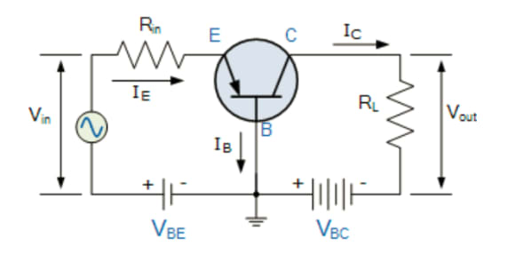
Image source: www.electronics-tutorials.ws
Configuring the circuit to have a common emitter will result in both current and voltage gain.
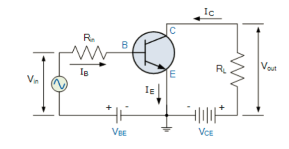
Image source: www.electronics-tutorials.ws
Finally, configuring the circuit like so to have a common collector there will be a current gain but no voltage gain.

Image source: www.electronics-tutorials.ws
FET
A Field Effect Transistor is a three-terminal unipolar semiconductor with very similar characteristics to BJTs. There are two main types of FET: a Junction Field Effect Transistor (JFET) and a Metal Oxide Semiconductor Field Effect Transistor (MOSFET). When learning about FETs and comparing these to BJTs, the first noticeable difference is the denotation of the three terminals. For a BJT we have a Collector, Emitter and Base, while for a JFET we have a Drain, Source and Gate.
(E) Emitter > (S) Source
(B) Base > (G) Gate
(C) Collector > (D) Drain
For a MOSFET there is an additional ‘substrate’ terminal which isn’t normally used as an input or an output connection but instead is used for grounding the substrate.
(E) Emitter > (S) Source
(B) Base > (G) Gate
(C) Collector > (D) Drain
> (SUB) Substrate

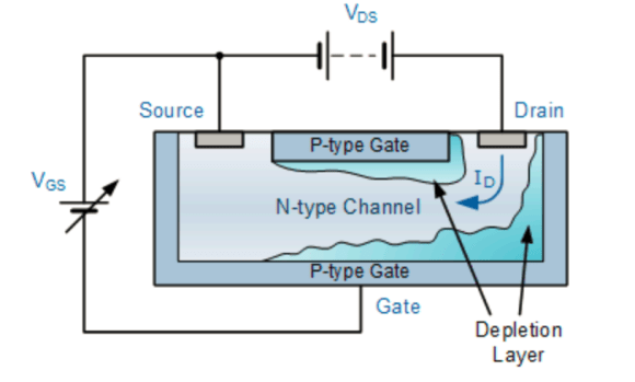
Once again, like BJTs, FETs use a specific denotation to describe the physical arrangement of their semiconductor compositions. FETs don’t have any PN junctions in the current carrying path, and instead, they have a ‘channel’ between the Drain and Source terminals made of either a P-type or N-type semiconductor. The type of semiconductor used determines whether this is a P-channel FET or an N-channel FET.
The gate of the MOSFET is electrically isolated from the conductive channel, hence why they are occasionally referred to as Insulated Gate Field Effect Transistors (IGFET). This isolated layer is most commonly made from a metal oxide semiconductor, which is where we get MOSFET from.
Some of the advantages which FETs have over BJTs are;
• Lower power consumption
• Lower power dissipation
• Smaller packages available
• High Z
These advantageous characteristics make FETs ideal for use within Integrated Circuits (ICs).
Further into the second semester, I look forward to going into more detail with MOSFETs and their two modes, as well as other transistor configurations such as Darlington Pairs.