Assembling & Debugging RC2014
Follow article
 Dave from DesignSpark
How do you feel about this article? Help us to provide better content for you.
Dave from DesignSpark
Thank you! Your feedback has been received.
Dave from DesignSpark
There was a problem submitting your feedback, please try again later.
Dave from DesignSpark
What do you think of this article?
A look at each RC2014 module, construction and debugging.
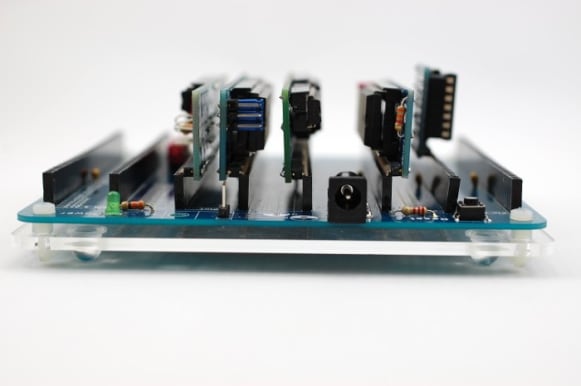
This kit is fantastic for anyone who enjoys soldering; with over 600 solder joints it isn’t really a kit which can be assembled in half an hour – unless you have the ability to solder like The Flash! All of the solder joints are through hole and there are no SMT components. Although the kit isn’t complicated to assemble, I think that with over 600 solder joints it becomes obvious that some soldering experience is required and it isn’t designed for a complete novice.

As I mentioned in RC2014 Modular Computing,I feel separating the components into bags for each board is the best way to start and once you’ve done this it’s fairly straight forward what goes where. The only thing which needs to be checked is the resistor and capacitor values. Since starting the project there is now an assembly guide available online which gives more guidance as to what goes where on each board.
I opted to purchase the backplane upgrade kit also which enables this to accommodate eight instead of five daughter boards, so additional modules such as digital I/O and Raspberry Pi Zero Serial Terminal can be added at a later date.
Full Backplane 8 Kit

There are 8 rows of 40 SIL pin header sockets on the backplane which up to eight daughter boards can be plugged in to. Each pin is connected to the bus for the Z80, including: 16 address lines, 8 data lines, Tx, Rx, 5v, GND, Reset and Clock.
In addition to the connections mentioned above there were also another 6 which I hadn’t come across before: M1, INT, WR, RD and IORQ. With a little bit of reading up on the Z80 processor I found out that:
IORQ – Input/Output Request pin, this is an output, active low and tristate (ON/OFF/HI-Z). When active this indicates that an address bus holds a valid address for reading or writing a digital I/O device.
M1 – Machine cycle pin, this is an output pin which is active low. When M1 and IORQ are both active this indicates an interrupt acknowledge cycle.
RD – Read pin, this is an output, active low and tristate. This pin indicates that data is ready to be read from a memory or I/O device to the CPU.
WR – Write pin, this is an output pin which is active low and tristate. This pin indicates that data is going to be written by the CPU data bus to a memory or I/O device.
INT – Interrupt Request, this is an input pin which is active low and also requires a pull-up resistor. This is generated by I/O devices and is honoured at the end of the current instruction, proving that the software-controlled interrupt flip-flop (IFF) is enabled.
A full BOM for the Backplane can be seen below. Assembling the backplane was pretty straight forward – I would advise using Blu-Tack to hold the 40 way SIL sockets straight:
- RC2014 BACK8 PCB
- 2.1mm Power Jack
- 8 x 40 Way SIL Socket
- 8 x 100nf capacitor
- Tactile Switch
- 2k2 Resistor
- 3mm Green LED
- 330R resistor
Clock/Reset
The clock module provides the system clock for the CPU and ACIA (Asynchronous Communications Interface Adapter). A clock can either be based on a crystal or an RC (resistor capacitor) circuit and in computing a crystal is predominantly used as they tend to be far more accurate.

Here the push button can be mounted onto the clock module or on the backplane and this is down to personal preferance. The BOM for this module is as follows:
- 8 pin RA Header
- 14 pin narrow DIL socket
- 74HCT04
- 7.3728 Mhz Xtal Crystal
- 22pf ceramic cap
- 1M resistor
- 1k resistor
- 2k2 resistor
- SPST Push Switch
Serial I/O
This is a method of communicating between devices – generally a computer and peripherals, sending one bit of data at a time. This can be used with the RC2014 to connect a terminal or terminal emulator software.
This daughter board consists of:
- 36 pin RA Header
- 24 pin wide DIL socket
- 14 pin narrow DIL socket
- MC68B50 ACIA
- 74LS04
- 6 pin header
- 2 pin header
- 2k2 resistor
Switchable ROM

With switchable read-only memory the RC2014 is designed in a way which means the 64k ROM is divided into eight 8k sections. Depending how the pin headers are jumpered this allows you to switch between the sections of the ROM. Doing this means that you can essentially treat this as eight separate ROMs. The complete module consists of:
- 32 pin R/A header
- 28 pin wide DIL socket
- 14 pin narrow DIL socket
- 27C512 EPROM or similar
- 74LS32
- 3 x 3-pin header
- 3 x jumper
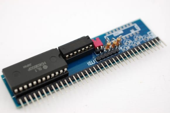
Z80 CPU

The RC2014 Central processing Unit is the section which carries out the instructions within the program. This module is a simple 8-bit Z80 microprocessor which was first developed in the 1970’s and was widely used in home computing in the 80’s and is the basis of the RC2014. When it came to assembling the CPU the assembly guide said to make a solder link across WAIT, BUSRQ and NMI – instead of doing this with solder I decided to use some pin headers which I had in the workshop and then use some jumpers to make this connection. To assemble the Z80 CPU the required components are:
- PCB
- 34 pin R/A header
- 40 pin wide DIL socket
- Z80 CPU
- 3k3 resistor
RAM

The 32K random-access memory is a single chips which provides memory to the CPU. To complete assembling the RAM module the following components were required:
- 34 pin RA Header
- 28 pin wide DIL socket
- 14 pin narrow DIL socket
- 74LS32
- 74LS04
- 62256 RAM
Serial Keyboard
In addition to the Full Monty Kit I also purchased the serial keyboard, which uses an ATMEGA328-PU. I knew the ATMEGA328 used on the keyboard didn’t have enough I/O pins for all 41 switches, so I wondered how this managed to read all these switches as inputs. I came across multiplexers a few months back and wondered if one of these had been used but I couldn’t see one on the PCB or the schematic. At this point I came across keyboard multiplexing and how this works, which all made much more sense. Keyboard matrices work like a grid and I found a really good online description available here.
Keyboard multiplexing means that based on where the grid is pressed you can tell which inputs were activated, meaning less inputs are required. For example, imagine numbers 0-5 along the Y-axis of a grid and letters A-E along an X-axis, only A, B, C, D, E, 0, 1, 2, 3, 4 and 5 would be the 11 inputs on the microcontroller but by crossing these it enables you to have 30 inputs; if A and 5 were detected as activated at the same time on the ATMEGA this would mean that the button located where A and 5 cross was activated.

Assembling the keyboard wasn’t difficult, just time consuming. Alone this PCB has over 200 solder joints with the following components:
- RC2014 Keyboard PCB
- 6 pin RA header
- 28 pin narrow DIL socket
- ATMEGA328
- 16Mhz Xtal Crystal
- 2 x 22pf ceramic cap
- 10k Resistor
- 100nf capacitor
- 41 x Tactile Switch
- 8 x 1N4148
Testing
At this point I could finally test the assembled kit. To power the modules I connected serial to 5V via a USB UART.

When I had powered the board the LED on the backplane didn’t illuminate. Initially I assumed I had a short somewhere on the backplane so gave the board another visual inspection. I couldn’t see any shorts, so I checked the voltage supply to the board with a multimeter. When I tested the backplane it was being supplied with 5V DC and the only reason I could think of as to why the LED wouldn’t be illuminating is that there must be some kind of fault with it.
I then checked the power to the LED, which was reading 5V at the cathode and 0V at the anode. At this point it confirmed my suspicion that the issue wasn’t the backplane but that I had soldered the LED in backwards. I soon realised that because there were no silkscreen on the PCB to indicate the orientation of the LED that I had just assumed that the square pad would be for the anode, as it usually is with other polarised components such as electrolytic capacitors – silly mistake. Ill be sure to remember to check the pads with a multimeter next time before I soldering in a component which I’m not 100% sure of the orientation of.
The problem was quickly resolved by de-soldering the LED and orientating it the correct way, following this I powered the board via serial I/O once again and the LED illuminated as it should.

To proceed with testing I connected to the RC2014 via the Minicom terminal emulator running on my laptop. When connected nothing came up in the program and there was no sign of anything being output to the terminal emulator. This wasn’t what I expected to see.
I wanted to rule out any shorts on both the backplane and the rest of the modules, so I visually inspected the solder joints before re-flowing most of these to ensure a proper connection had been made. Once again when connected up to Minicom nothing was displayed.
Debugging
Since I’d checked the solder joints and all the connections I wasn’t too sure why I didn’t get anything displayed in Minicom. At this point I thought this would be a good idea to check each of the modules. I began by checking the power supplied to each of the slots and across the mounting holes for the voltage regulator, and here the readings were exactly what I would have expected them to be. Following this I checked the current draw of the modules with a bench power supply and received a reading of 35mA when all the boards were plugged into the backplane. After confirmation with the designer of RC2014 I was confident that this reading was sufficient.
I then connected the clock to an oscilloscope and the square wave wasn’t quite as square as I would have expected. Bearing in mind that this was quite an old scope I then decided to use a much newer and higher end oscilloscope to test the clock module. I connected the scope probes to GND and Clock on slot 1 and then proceeded to take a measurement.

Using the higher end scope gave me a much cleaner signal and the clock looks much more like a square wave on this piece of equipment. I also checked the clock module in the backplane on its own without any other boards and the waveform was pretty much the same as before.

To be 100% certain I wanted to check the current drawn form each of the modules in the backplane, the backplane on its own and then finally all the boards in the backplane together. The results were are follows:

I would have expected the current drawn from each board to total the measured current drawn from all the modules in the backplane together, as a calculated of 53mA and a measured of 35mA is a 51.4% increase compared to the measured result. Because of this I wanted to be sure the readings obtained from the bench power supply were accurate, as the one I initially used for these readings is fairly old. To check this I once again took a set of readings from a more much more modern digital power supply which confirmed the original readings to be correct within 1mA, this was good enough for me.

I once again connected the completed RC2014 modules up via FTDI to Minicom and had no luck. I need to do some more debugging and probe deeper – hopefully in my next post I’ll have a working system where I will be able to take a look at its basic operation.
UPDATE 19/10/2016: Thanks to Spencer Owen for pointing out a descriptive error and also that the RAM and Rom chips are swapped. Upon inspection I soon realised this had happened because the "RC2014 BASIC" sticker had been placed on the RAM and I would have expected to see this on the ROM - I'll be sure to check the component part number against the silkscreen in future! Please note all relevant images have been changed to illustrate the correct chip in each board.