First PCB Project - Fourth Time Lucky!
Follow article
 Dave from DesignSpark
How do you feel about this article? Help us to provide better content for you.
Dave from DesignSpark
Thank you! Your feedback has been received.
Dave from DesignSpark
There was a problem submitting your feedback, please try again later.
Dave from DesignSpark
What do you think of this article?

Resolving problems with the light theremin and success at last.
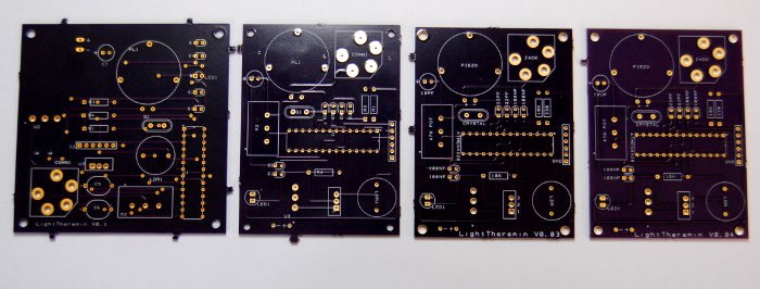
I wrote previously about my first ever PCB project and how the initial boards that came back had errors that needed to be addressed. It took a few more attempts before I finally achieved a working design! By no means was the circuit complicated, however, it would perhaps have made sense to start with something much simpler.
I was pretty much thrown in at the deep end; I referred to a lot of web tutorials to learn to use DesignSpark PCB and had no previous experience with the fabrication process.
Version 0.2
After the faults with the first version I spent a considerable amount of time when designing the second to make sure there were no mistakes. I confirmed that the DesignSpark PCB schematic matched the original hand drawn one, and the PCB layout electrically matched these.
I played about a lot with the placement of tracks on layers to eliminate any unnecessary vias. I also repositioned a lot of the components to make the board much more compact and neater.

The very first thing I noticed when the boards came back was that the drills were significantly smaller than the previous boards, to the extent that not all of the components would fit.
I thought this must have been a fault with fabrication, however, upon review with the manufacturer support team it appeared I had uploaded the wrong drill file.

I had uploaded drills.gbr instead of drills.drl, thinking all the extensions should be Gerbers, but unfortunately I was wrong.
Fixing the drills
To resolve this I manually drilled out the holes myself using a pillar drill. One problem with doing this is that it broke the connections between the top layer and the bottom layer. To fix this I had to run quite a lot of solder between the layers.
When the board was assembled I programmed the ATMEGA with the light theremin sketch and found the LED illuminated, both when the programming cable was attached and when it was connected to the battery. So at first impression I thought everything was OK.

When powered up this then made the piezo sound. I then began covering and uncovering the LDR, however, this made no difference to the pitch. The potentiometer worked as it altered the volume of the piezo.
Process of elimination
At this point I used a multimeter to check the ATMEGA was receiving the correct supply voltage.
I considered the possibility that there may be a problem with the ATMEGA and so to check this I used serial.print to check this was outputting as it should.
void setup() {
Serial.begin(9600);
}
void loop() {
Serial.print("Hello world");
delay(1000);
Serial.print(":)");
delay(1000);
}
I opened the serial monitor and the ATMEGA was outputting “Hello world” as expected.
I then wanted to rule out that there wasn’t a fault with the piezo, so I connected an external amplifier. I still received the constant dull buzzing noise with no change in pitch.

At this point I wasn’t entirely sure what could be wrong with the board, so I decided to refer back to the schematics. I noticed that in the very original hand drawn schematic there was a resistor which had been connected wrong. The ATMEGA A0 pin was connected directly to GND, instead of via a 10K resistor, which was also connected to Vcc through the LDR. This explained why the piezo only output a constant dull tone, since A0 was tied to GND.

Correcting mistakes
To resolve this I corrected the mistakes in the original hand drawn schematic and proceeded to make the same changes in the DesignSpark PCB one.
For the third version of the board I didn’t use auto-router; I manually laid out all the tracks myself to reduce the possibility of mistakes. This also made the board look a lot neater.
Once the board had been laid out I sent the design to fabrication.
Receiving the V0.3 boards back from fabrication
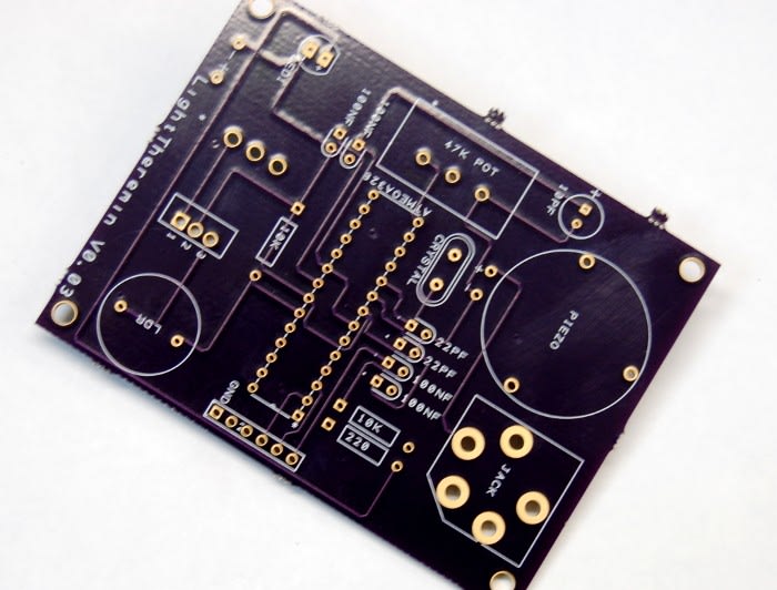
Upon inspection of the board I noticed that on the top layer there were two tracks overlapping! I checked the PCB files multiple times and couldn't seem to work out how this had happened.
Rerouteing tracks
To correct this problem I cut one of the overlapping tracks and rerouted this on the reverse of the board using wire. I then programmed the ATMEGA and powered the board up, to find that everything worked as expected!

At this point I re-checked the board layout in DesignSpark PCB and everything looked fine, so I re-generated the Gerbers. After viewing these in a Gerber viewer I confirmed that there were no errors and those tracks didn’t overlap. It appears I must have made an error uploading files previously, such as uploading an older version of the files.
So I once again sent of a set of Gerbers for manufacturing!
Fourth and final version
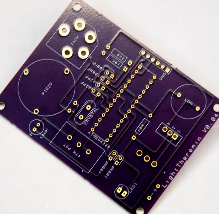
After assembling version 0.4 I was over the moon to find it worked as it should!

In the initial assembly of this version I made a slight mistake in that I connected the potentiometer the wrong way round, meaning turning it anti-clockwise would increase the volume. I resolved this by de-soldering the outer connections and swapping them.
With a working PCB assembly, I next used Inkscape to design a simple case that was laser cut from acrylic.

After four attempts and some silly mistakes along the way it gave me a huge sense of achievement finally having a working design!
More lessons well learned
In creating my first ever PCB project I have learned many invaluable lessons. In future with PCB design projects I will be sure to bear in mind:
-
Check and double check the original schematic drawings and make sure they are all electrically correct. If they are not correct at this point you will end up with design faults.
-
Print out your final PCB layout at actual size and lay out all the components to make sure they fit on the board and that all the footprints are correct.
- Ensure when uploading files to fabrication they are in the right format, with the right extension.
When next designing a PCB I will take into account all the mistakes I made in the process of getting a working design this time! Fingers crossed and hopefully next time I'll get it right first time.