Hand-made circuit board by Heat transfer printing method
Follow article Dave from DesignSpark
How do you feel about this article? Help us to provide better content for you.
Dave from DesignSpark
Thank you! Your feedback has been received.
Dave from DesignSpark
There was a problem submitting your feedback, please try again later.
Dave from DesignSpark
What do you think of this article?
This blog is the translation of “热转印法手工制作电路板” written by hao zhu
The heat transfer printing method is one of the simplest among amateur methods. This method is most commonly used right now by electronic enthusiasts. It takes advantage of the anti-corrosion characteristics from the laser printer toner. Some features also includes lesser time needed for printing the boards (usually 20 minutes), high precision (width for wiring and spacing is 15mil and 10mil), low cost and so on. I will now share my technique on making the board by heat transfer printing method.
Tool:
- Printer
- Heat Transfer Machine
- Drill Floor
Material:
- Copper Clad Laminate
- Transfer paper
- Etching solution
- Sandpaper
- Paper tape
Step:
First of all, complete the schematic and PCB layout using DesignSpark PCB.
Print the PCB layout onto the transfer paper. Note that it should be printed layer by layer and simply print the top layer (Mirror image) and the bottom layer (For single layer board just prints the wiring layer).
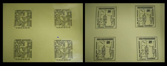
Out of the 4 printed layouts, select the clearest sample and cut it along the edge, then use the paper tape to stick the sample onto the board

When making a double layer board, align the holes of the top and bottom layer paper accurately. Before proceeding, it is recommended to fix the first layer with pins as shown in the picture below. The other layer is required to be fixed carefully based on the location of positioning holes (For the single layer board, directly fix the transfer paper with the paper tapes.)
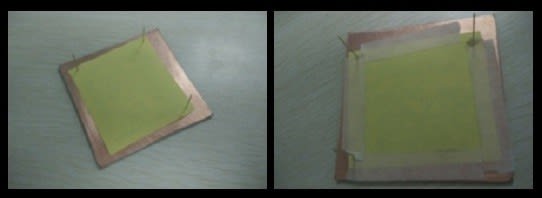
With help from the heat transfer machine, transfer the toner from the sample to the Copper Clad Laminate. Observe the whole process of the heat transfer. In case of broken tracks, sign pen can be used to connect or you can just perform the following steps.

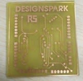
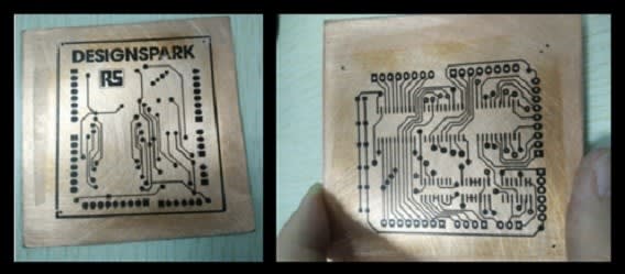
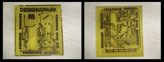
Complete PCB board by Heat transfer method as shown below.
Put the Copper Clad Laminate into the etching solution and wait for the Copper Clad Laminate to be etched.

Use a tweezer to clamp the Copper Clad Laminate out of the etching solution and clean it using water.
Use sandpaper to remove all the ink and you will only have copper wires left on the PCB Board.

Drill the holes
Solder the electronic components.
Testing of the board
TIPS:
1. Select an appropriate width for wiring and spacing on the PCB board and it should be adjusted according to the limits of the actual machine to print the board.
2. Vias and pads cannot be shared. There is no eletcroless plating copper in the inner layer of Copper Clad Laminate, so it requires a separate process of the vias.
3. The number of PCB positioning holes are preferably three, located in three corners. (The principal of three points defining a plane. In the meantime, it avoids the possibility of inverted positioning of the top layer and bottom layer.)
4. When fixing the transfer paper, ensure to use the paper tape! Some tapes which are not heat resistant will be melted in the transfer machine.
5. If you want to accelerate the corrosion rate, the solution can be used with warm water, while gently shaking the copper clad laminate or the corrosion container.